Project: A combined On Board Charger (OBC) + DC-DC module for super car
Timescale: A working week
Scope of work:
A high voltage combined OBC and DCDC module has experienced radiated emission during the pre-compliance EMC testing. The client’s customer’s pre-compliance result also shows similar spectrum profile in the frequency range of interests. The scope of this work includes:
- Review the DC-DC module and identify EMC design areas of improvement
- Review the radiated emission failures and provide cost-effective solutions
- Any other recommendations that could benefit the system power and signal integrity
The client is a Silicon Valley based company specialised in making smart motors, the branch is their UK branch, their customer is a super car company in the UK.
Since it is an isolated DC-DC converter, therefore we present the coupling mechanism here:
While the high slew-rate voltage of the primary MOSFET drain terminal is the main source of CM noise, the transformer and its parasitic capacitances are the coupling channels through which conducted EMI can propagate from primary to secondary and through the impedance from output circuit to chassis. The dominant CM current path (shown in Figure 1) is from primary to secondary across the transformer and through the impedance from the output circuit to chassis. Using a small switch-node copper area, connecting the MOSFET heat sink to HV_0V, and avoiding switch- node full vias to the bottom side of the board are three techniques that diminish the coupling from the MOSFET drain to chassis.
CM noise is mainly caused by displacement currents within the transformer interwinding parasitic capacitance and the parasitic capacitance between the power switch and chassis.
Each switching event excites damped voltage and current oscillations between switch and diode parasitic capacitances and transformer leakage inductance. The ringing depends on the primary-side leakage inductance resonating with the MOSFET output capacitance plus the transformer primary interwinding capacitance.
Similarly, the secondary stage voltage ringing relates to the secondary-side leakage inductance resonating with the MOSFET capacitance and secondary interwinding capacitance. The overshoot and ringing have high transient voltages (dv/dt), so any capacitive couplings to the chassis lead to induced displacement currents and CM noise.
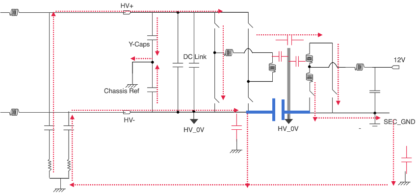
Adding a capacitor between the primary ground (HV_0V) and the secondary ground (shown in blue in Figure 1) will shunt the secondary side RF current back to the primary side, this means less current going through the secondary ground and chassis capacitance, less common mode current, i.e reduced radiation. The capacitor needs to be a safety-rated capacitor selected with a voltage rating of 1 kV or higher, well above the required isolation voltage specification. However, galvanic isolation is compromised if this capacitor becomes shorted during a fault condition. Also, the capacitor can conduct excessive current if the SEC-GND connection has a high CM voltage swing relative to the primary, for example in high-side gate-driver bias-supply applications.
Other techniques to reduce the common mode coupling path of a transformer are adding balanced capacitor, adding flux cancellation winding, or adding more shields. These techniques can be found in our training course.
The biggest problem of the design is its chassis reference design. As mentioned before, the noise source has a low impedance connection to the chassis (via parasitic capacitance between the MOSFETs and the chassis). Unless even lower impedance path is provided, common mode noise will travel on the testing ground plane and back to the noise source via cables. This noise will be picked up by measurement LISN, the cables will radiate (as it was observed during the pre-compliance test).
A chassis plane (solid and continuous) designed on the PCB with a good electric connection (multiple screw points) is a way to provide low impedance path. However, the current design suffers the following:
- No low impedance chassis reference on the PCB.
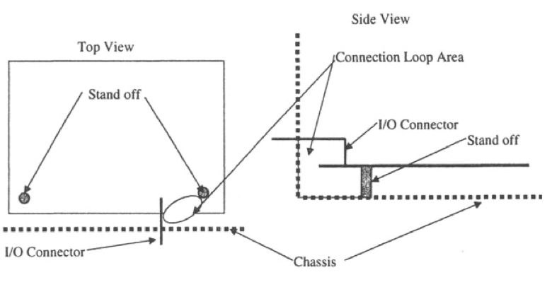
- The mounting screw points are not directly on the chassis, but rather, via posts (50mm long)
The following diagram demonstrates the problem of mounting PCB on posts. Increased loop area means increased parasitic inductance. When frequency increases, the impedance increases.