Project: A package of EMC troubleshooting work on an EV charger
Time scale: 3 working days including a 2-day troubleshooting and 1-day technical report
Scope of work: The device under test (DUT) is a charger for electric vehicles. Previous EMC test results show that the DUT fails conducted emission, radiated emission and electric fast transient (EFT) tests.
For this work, we propose on-site troubleshooting activities combined with review work. Scopes of work are therefore defined as below:
- To perform an EMC on-site testing using test equipment, with a particular focus on the conducted emissions, radiated emissions and EFT.
- Carry out fault finding and recommend cost-effective production fixes. We will also assess the EMC performance of the system under test during the visit.
- To document the troubleshooting and lesson learnt in a written format.
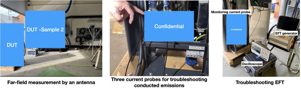
An electric vehicle (EV) charging station failed the conducted and radiated emission tests in the EMC test chamber. In this case, the device under test (DUT) is a 60-kW unit powered by a three-phase power supply. The high cost of renting the test facility and the transportation of a large installation make EMC troubleshooting in the test chamber costly.
Testing and troubleshooting the DUT at the factory site proved to be a cost-effective solution for the manufacturer. A three-phase LISN rated for 75Amp is hard to rent (in the UK) and would require a large isolation transformer to prevent it from tripping the circuit breaker at the customer’s factory site. Therefore, a pair of matched RF current probes were used as the primary troubleshooting tool for conducted emissions. The concept of using a pair of matched current probes was first introduced in [1]; in our case study, the matched pair ensures simultaneous measurement of the RF current in the subsystems of the DUT.
Results
CM noise in the low-frequency range
The high level of CM noise in the DUT contributed to the conducted emission failure. A clear understanding of the noise propagation path is needed to solve the noise issues.
Whether the noise is DM or CM depends strongly on the coupling path to earth (in this case, it is the true earthing point as the RF reference). In a single-phase power system, products whose Live and Neutral wires are double insulated do not require earth wire connection, so the capacitance to earth is extremely low. Therefore, the impedance to the earth is mostly dominated by the impedance of the artificial hand.
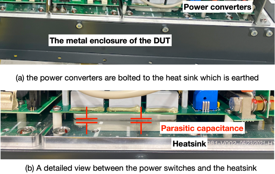
Industrial equipment (often powered by a three-phase supply) is usually earthed and has a sizeable earthed heatsink with the power switching devices bolted to it, this forms a high capacitance from the noisy node of the switching converter to earth as shown in Figure 3. When the switches are turned on and off at a fast speed, a large amount of CM noise is introduced because of the Cdi/dt. A 10 nF capacitance from the transistors to earth is not uncommon, at 200 kHz, the impedance is only 80 Ω.
Understanding the CM noise propagation path provides solutions to the issue. One way of reducing the noise is to reduce the capacitance from the noisy node to the earth. This can be done by floating the heatsink, though this approach often requires sufficient air-cooling in the system.
Sometimes, a shield between the transistor and the heatsink can work well, which worsens the thermal conduction path. This, again, demonstrates the trade-off that a design engineer often faces between efficiency and EMC. Other times, a choke/ferrite in the earth line helps, but this can make radiated noise worse.
Troubleshooting and problem fixing
Once the CM noises were measured before and after the filter, the same current probes were then used in the critical common mode propagation paths in the DUT including the AC cable of the rectifiers, the DC link bus wires, control cables, ethernet cable links and so on. This is a technique we call “CM noise mapping”. This exercise identified the DC link as a “hot area” where a significantly high level of CM noise was observed.
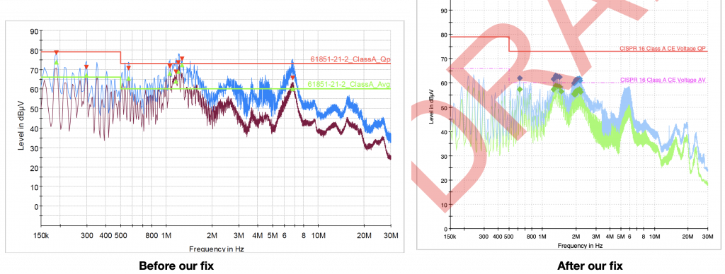
Two capacitors from the DC bus wires to the heatsink were placed to reduce the noise, the temporary fix (for troubleshooting only, not the final implementation) was shown in Figure 4, where the capacitance value of each capacitor was 330nF, it can be seen that the noise measured behind the filter was reduced, especially at the frequency points of interest (180kHz, 300kHz and above). The touch current was also checked to ensure no excessive leakage current was caused by the extra capacitance added to the system. Subsequent tests in the EMC chamber showed a pass for the conducted emission tests when a properly designed capacitor PCB was retrofitted to the system.