Troubleshooting Radiated Emissions of a Smart Scale
Timeline: 1 working week
Scope of Work: The client’s product encountered radiated emissions issues, including both broadband and narrowband emission failures. The client, a Silicon Valley company, sought our assistance after considering several EMC consultants. Our task was to rectify the radiated emissions problems to ensure the timely market launch of their product.

Storyline: The pursuit of fitness and longevity is a common human aspiration—to live a longer, healthier life. In line with this goal, our client, a Silicon Valley-based company, developed a smart scale that provides more than just weight measurements; it offers valuable health-related insights.
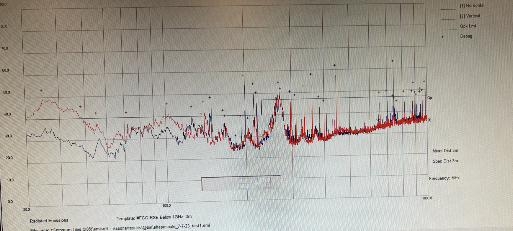
However, the intelligence of this smart scale relies on sophisticated electronic components, including a Wi-Fi module—an off-the-shelf component. During testing, this module generated third, fifth, and seventh harmonics that exceeded the radiated emission limits. In addition to these narrowband failures, there were also instances of broadband emission failures in radiated emissions testing.
Addressing the broadband radiated emission failures proved relatively straightforward; the placement of a ferrite core on the ribbon cable mitigated the issue. However, tackling the narrowband noise generated by the Wi-Fi module presented a more formidable challenge.
The root of the problem lay in the fact that both the off-the-shelf Wi-Fi module and the System on Chip (SoC) module had unknown internal ground routing configurations. The suboptimal ground designs of these chips meant that noise control during communication between the two chips primarily depended on the motherboard design. The communication between the chips relied on the Serial Peripheral Interface (SPI) communication protocol, utilizing four lines in total.
Given the narrowband nature of the failure, it was evident that the clock frequency and its associated odd harmonics were responsible for the emission test failures.
Initially, we considered implementing controlled impedance on the main PCB to reduce reflections. However, past experience indicated that this approach had limitations. The SPI bus extension, featuring command and four parallel data lines, was mainly push/pull I/O at 3.3V up to 25MHz or 1.8V up to 50MHz, making it an unbalanced, high-impedance input with low-impedance outputs. This rendered controlled impedance somewhat meaningless. The ideal solution involved adding a series resistance near the driver, such as 22 ohms, to dampen reflections without compromising signal integrity. Balancing the drive strength and series resistance was crucial to avoid rounding off signal edges or inhibiting bus functionality. Additionally, careful consideration of microcontroller pin drive strength and slew rate was necessary. Employing small capacitors as filters or BLM-type Murata ferrites were other viable options. The trace impedance, while typically around 50-100 ohms, was less critical, with the focus on damping the bus and benefiting from the Faraday cage effect of buried coplanar traces.
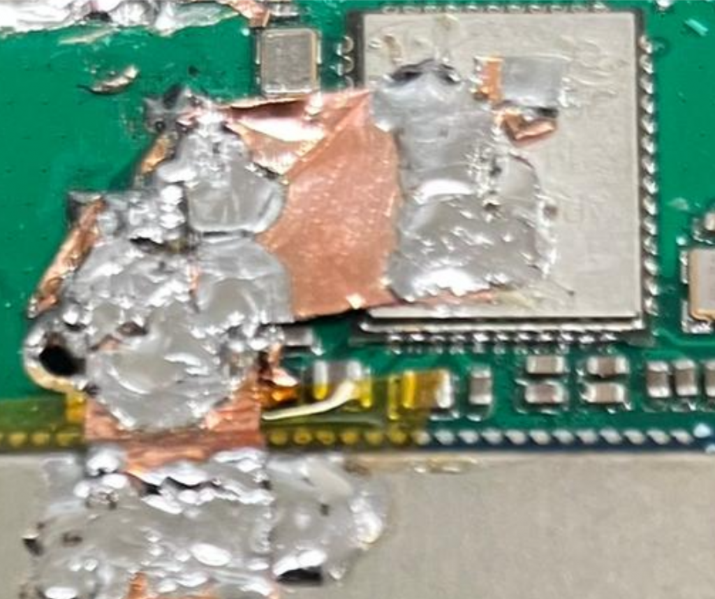
In this case, we opted for an on-board shielding solution, which proved effective in resolving the issue. This solution required the manufacturer to design a PCB board accordingly. We are pleased to report that they subsequently passed the EMC test. We wish them the best of luck in their endeavors as a startup, understanding the challenges they face in the industry. Good luck!