Project: Emissions of an Industrial Pump
Timescale: Two working days
Progress:
- During the investigation process in the client’s pre-compliance chamber, two units were thoroughly examined, with particular emphasis on conducted and radiated emissions.
- The manner in which the earth wire is connected to the chassis plays a significant role in determining emissions.
- The power factor correction (PFC) circuit and the motor drive circuits were identified as the primary sources of noise in the device under test (DUT). Each of these sources contributes to different frequency ranges in the profiles of conducted and radiated emissions.
- For applications like these, a well-designed filter becomes crucial. Its strategic placement is vital to controlling and minimizing coupling effects.
- Maintaining proper “grounding” is essential for achieving a low noise profile in the client’s product lines. Three main forms of “grounding” are pivotal: earth (chassis/motor frame), HV (the high voltage DC link, where the negative terminal of the electrolytic capacitor is connected), and low voltage ground (also referred to as GND_ISO in their schematics).
To locate the noise source, it is essential to understand the relationship between the time domain and the frequency domain. A resonance peak observed in the frequency domain can also be observed in the time domain.
Here, we present a case study demonstrating how to locate the noise source in a motor drive circuit. In Figure 1, we can observe a 10 MHz resonance peak in the conducted emission results. The motor drive unit comprises an AC-to-DC power converter stage (with active power factor correction), a DC-to-DC power converter stage, and a DC-to-three-phase motor drive circuit. It is crucial to identify which circuit in this product is responsible for the 10 MHz “hump.”
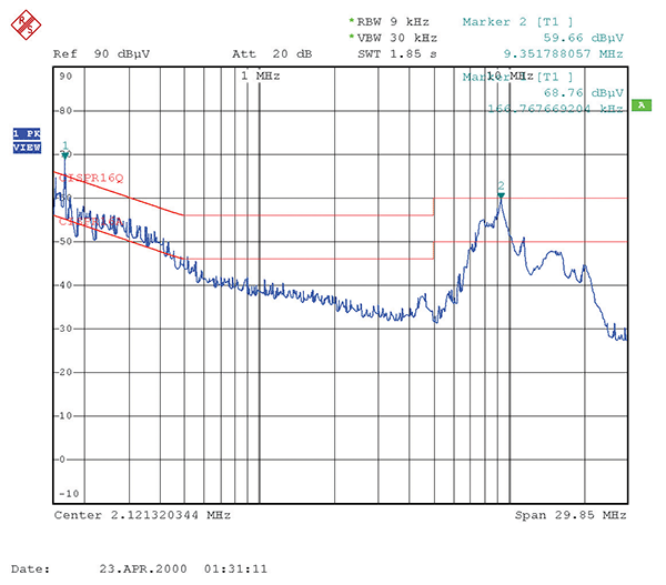
Figure 2 illustrates the setup for locating the noise source. An RF current probe is positioned on the mains cable and connected to the 50-ohm input of an oscilloscope (channel 2 in this case). Channel 1 of the oscilloscope (also configured to be a 50-ohm input) is connected to a near-field probe. The measurement result from the RF current probe serves as a stable trigger. By moving the near-field probe to accessible parts of the system, we can compare the noise signal picked up by the near-field probe with the RF current probe signal. The noise signal picked up by the near-field probe can be in phase or anti-phase compared with the RF probe.
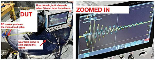
After zooming in on the noise signal captured by the RF current probe, we can observe the 10 MHz ringing on the oscilloscope. If the near-field probe also displays a similar ringing pattern, we can conclude that the noise source has been located. In Figure 2, it is evident that both channels exhibit a 10 MHz ringing when the near-field probe is positioned near the PFC circuit.
Once the noise source is identified, we can proceed to develop strategies for mitigating its impact. In this case, the solution involves optimizing the RC snubber circuit of the PFC circuit, which utilizes a SiC MOSFET. The high noise level experienced can be attributed to the SiC MOSFET. By implementing improvements to the RC snubber circuit, we can effectively reduce the noise generated by the PFC circuit.