Project: A Head Up Display (HUD) used in automotive application experienced both conducted and radiated emission failures
Timescale: Two working weeks
Scope of work:
An electronic circuitry that is used in a head up display (HUD) unit for automotive application has experienced EMI issues. Some pre-compliance EMC tests have been performed in the EMC test house, namely conducted and radiated emissions tests. The unit failed both tests.
The scopes of work are defined below:
- Design recommendations for fixing the conducted emission.
- Design recommendations for fixing the radiated emission.
- Other design modifications which will benefit future tests, such as immunity tests.
The client is a Cambridge based technology company specialised in visual technology, their client is a huge Japanese Tier-1 company that produces lots of parts for OEMs.
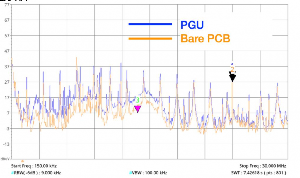
During the investigation stage, we have found that the emissions (both conducted and radiated) predominantly come from the switched mode power supply (SMPS). The SMPS has a ‘silent’ switcher which has a fixed switching frequency at 1.8 MHz. As a result, on the emission profile, we saw 1.8 MHz related noise dominating the spectrum. See pre-compliance test result in Figure 1.
The noise turns out to be both differential and common mode by nature, therefore, a quick fix like the one shown in Figure 2 sufficiently brought down the noise by about 20dB.
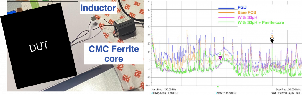
Of course, we cannot put these two heavy filters in a compact designed automotive product. So the next step is to fix the problem at the noise source. As mentioned, the SMPS is where the troubles are, so we need to fix that part. The approach we took to identify the noise source is by near-field probing, which is a powerful tool in the trouble shooting stage.
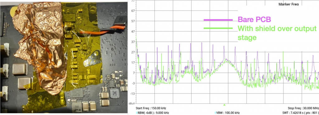
The SMPS has a big problem, which is that the output stage coupled so strongly with the input filter. Therefore, the originally designed filter, which is supposed to give about 60-80 dB attenuation in the frequency range of interests, failed to suppress the noise. In fact, it probably only had about 10-20 dB attenuation due to the coupling effect. In order to prove the point, one quick way is to shield the output stage, so that the coupling between the output stage and input stage is reduced to minimum. The shield we used is just copper tape. Note that in between the copper tape and the PCB, make sure to use Kapton tape to insulate the PCB. The copper tape also needs to be bonded to GND. Luckily, there is a local ground point that we could use (see top left on Figure 3, where the shield is bonded).
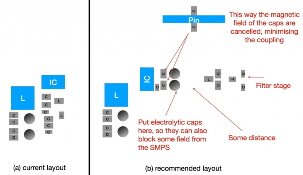
So we provided our layout recommendations as below
Design of Switched Mode Power Supply, especially the layout, is critical to passing the EMC standards. There’re many considerations engineers need to take when designing the SMPS. In Mach One Design, we help you overcome these design challenges so that you can get your design out of the door quickly. Contact us to learn more.